Service hotline: 18602717479

WeChat QR code

Service hotline: 18602717479
WeChat QR code
Service hotline:
0755-27208339
Tp:18602717479
Add:F6, BDG 5, RunDongSheng Industrial zone, Baoan district,Shenzhen,Guangdong
QQ:576498273
Email:info@e-lines.cn david@e-lines.cn
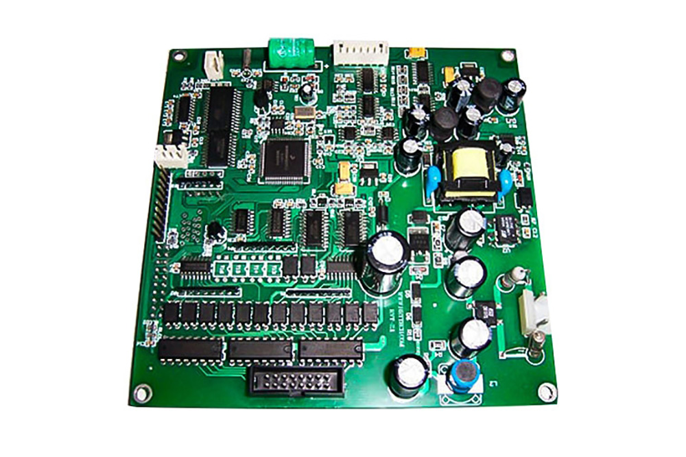
In fact, PCB circuit boards can be judged by their appearance, which is a relatively direct method. Mainly able to distinguish from thickness, light and color, weld appearance, etc.
1. Standardized rules for size and thickness.
The thickness of circuit boards varies according to the specifications, and customers can measure and view the thickness and standards based on their own products.
2. Light and color.
External circuit boards are covered with ink, which can provide insulation. If the color of the board is not bright and there is less ink, the insulation board itself is not good.
3. Weld appearance.
Due to the large number of parts on the circuit board, if the welding is not done properly, the parts are prone to fall off, which seriously affects the welding quality of the circuit board. It is very important to carefully identify the appearance of the circuit board and have a strong interface.
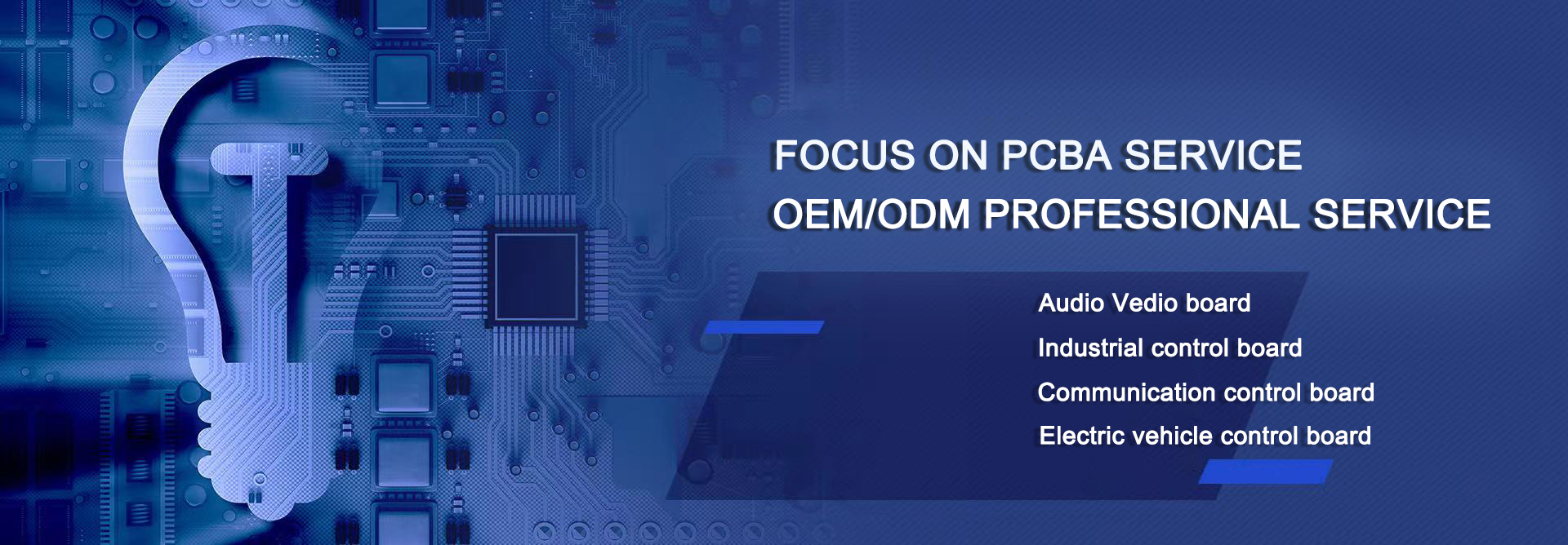
The characteristics of external assembly components in PCBA processing are as follows:
1. On the electrodes of SMT equipment, some welding ends do not have leads, while others only have very small leads; The spacing between adjacent electrodes is much smaller than the lead spacing, and the spacing between pins in integrated circuits is reduced to 0.3 millimeters; At the same integration level, the area of SMT components is relatively small, and the chip resistance and capacitance have now been reduced to 0.6mm0.3mm.
2. The SMT components are directly installed on the surface of the printed circuit board, and the electrodes are welded to the solder pads on the same side of the SMT components. In this way, there are no solder pads around the through-hole, greatly increasing the wiring density.
3. During the PCBA processing, the surface mounting process not only affects the area occupied by wiring on the printed circuit board, but also affects the electrical characteristics of equipment and components. There are no leads or the leads are short, reducing the parasitic capacitance and inductance of the element equipment, and improving the high-frequency characteristics, which is conducive to adding usage frequency and circuit speed.
4. Simple appearance, solid structure, closely attached to the exterior, enhancing reliability and impact resistance; During assembly, there are no bent or trimmed leads. When making printed circuit boards, the size and shape of the through-holes used to place components are standardized and reduced, and automatic placement can be achieved by using an automatic placement machine. This method has high efficiency, reliability, convenience for large-scale production, and low overall cost.
5. In the traditional sense of PCBA processing, externally mounted components do not have pins or short pins. The entire exterior component accepts a higher temperature, but the pins or endpoints of the exterior mounted component can accept a lower temperature during welding.

Telephone:18602717479
Service hotline:0755-27208339
Q Q:576498273
Email:info@e-lines.cn david@e-lines.cn
Address:F6, BDG 5, RunDongSheng Industrial zone, Baoan district,Shenzhen,Guangdong
Scan for more information
Add WeChat sweep the code