Service hotline: 18602717479

WeChat QR code

Service hotline: 18602717479
WeChat QR code
Service hotline:
0755-27208339
Tp:18602717479
Add:F6, BDG 5, RunDongSheng Industrial zone, Baoan district,Shenzhen,Guangdong
QQ:576498273
Email:info@e-lines.cn david@e-lines.cn
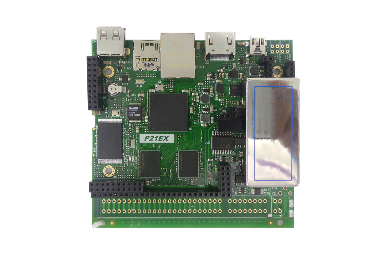
The holes on PCB circuit boards are generally divided into copper holes and non copper holes. Non copper holes are mainly used for positioning and installation, and are generally classified as larger holes with a diameter of 0.8mm or more. However, if there are through holes, the plug-in may be through holes. The common holes on PCB boards should be through holes (conduction holes), and the hole size of the plug-in hole is larger than the through hole size, usually above 0.5. According to the installation of capacitors, resistors, sockets, and other components. And the main function of the electric hole is to have a conduction effect, with a generally small aperture, commonly below 0.3. With the increase of fine boards, the functional requirements of the product increase, and the number of circuit board layers increases, the aperture also becomes smaller and smaller, with a small aperture of 0.1mm. Laser drilling is required.
The through-hole needs to have a conductive effect, and copper skin is needed inside to conduct. Therefore, the thickness, saturation, and quality of the copper in the through-hole naturally become the key factors in the later operation of the circuit board. Generally speaking, the thickness of the hole copper wall of PCB board is required to be between 10um and 20um, and products with higher current requirements may require a thickness of more than 25.4um. Because the hole copper is electroplated in the later stage, unlike the surface copper which comes with the raw material, the quality of the hole copper depends on the production and processing of the circuit board factory in the later stage. The length of electroplating time, the quality of electroplating line operations, and so on. Generally, saturated porous copper plates are required, and it is expected that sufficient time is given on the electroplating line as much as possible. Otherwise, simple formation of porous copper is not feasible, and the copper balls also require purity and haste, otherwise bubbles may form. If the copper hole is not functioning properly, it may cause a circuit board to break during later operation, or it may burn out.

Telephone:18602717479
Service hotline:0755-27208339
Q Q:576498273
Email:info@e-lines.cn david@e-lines.cn
Address:F6, BDG 5, RunDongSheng Industrial zone, Baoan district,Shenzhen,Guangdong
Scan for more information
Add WeChat sweep the code