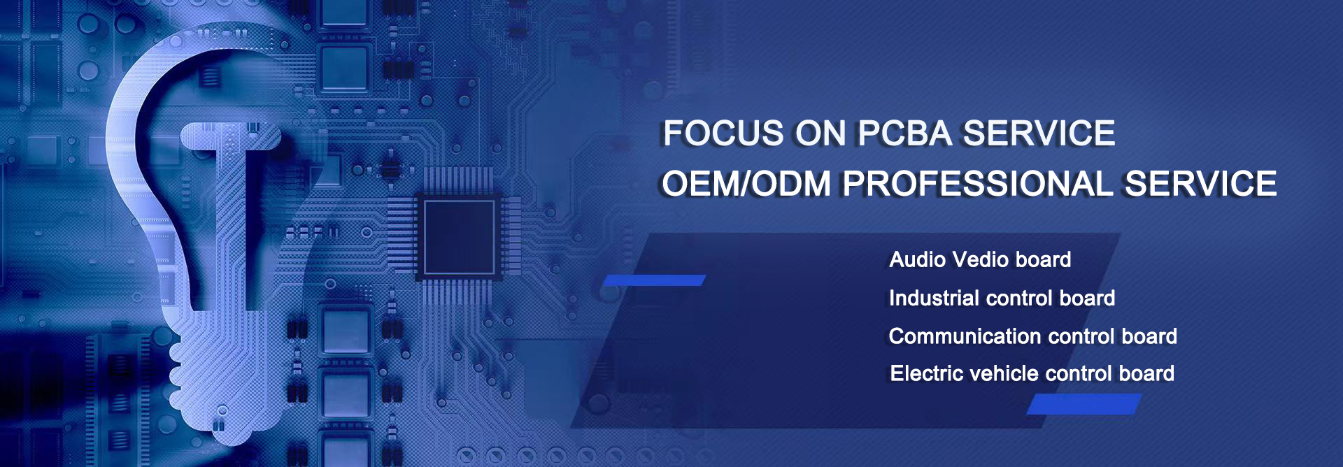
Service hotline: 18602717479

WeChat QR code

Service hotline: 18602717479
WeChat QR code
Service hotline:
0755-27208339
Tp:18602717479
Add:F6, BDG 5, RunDongSheng Industrial zone, Baoan district,Shenzhen,Guangdong
QQ:576498273
Email:info@e-lines.cn david@e-lines.cn
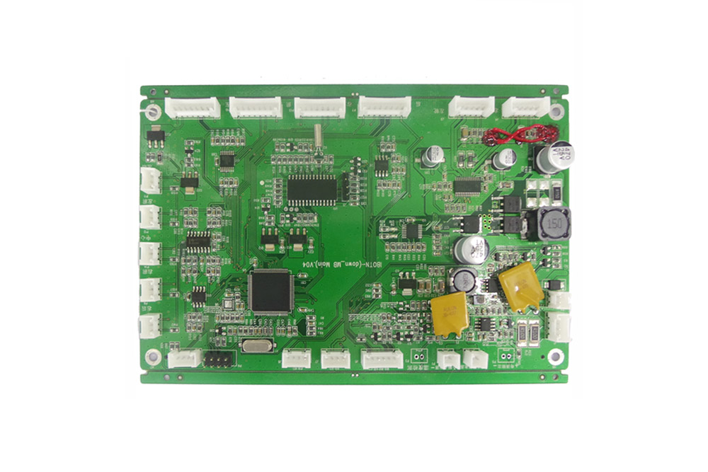
It is necessary to check the processed electronic products in SMT chip processing. Below, the editor of SMT chip processing factory will introduce the key points of SMT chip processing product inspection:
1. Quality requirements for component installation process
The installation of components should be neat, centered, and free from deviation or inclination.
The type and specifications of the components placed in the correct position should be correct; The component should not have short stickers, faulty stickers.
Chip mounted components are not allowed to have reverse mounting.
Installation of patch devices with polarity requirements should follow the correct polarity instructions.
2. Requirements for soldering process of components
The appearance of the FPC board should not affect the appearance of the solder paste, as well as foreign objects and traces.
The bonding direction of components shall be free of rosin or flux and foreign matters that affect the appearance and soldering tin.
The forming of tin points under the component is outstanding, without abnormal wire drawing or excellent phenomena.
3. Printing process quality requirements
The orientation of the solder paste is centered, without obvious errors, and does not affect the pasting and welding of the tin.
The printing solder paste is moderate and can be prominently posted without any shortage or excessive solder paste.
The composition of the solder paste is outstanding, and should be free from solder joints and unevenness.
4. Appearance process requirements for components
The bottom, surface, copper foil, wires, through-holes, etc. of the board should be free of cracks and cuts, which will not cause short circuits due to poor cutting.
The FPC board is parallel to the plane and has no protruding deformation.
The identification information characters are screen printed without ambiguity, offset printing, reverse printing, offset printing, double shadow printing, etc.
The outer surface of the FPC board should not expand bubbles.
The aperture size meets the planning requirements.

Telephone:18602717479
Service hotline:0755-27208339
Q Q:576498273
Email:info@e-lines.cn david@e-lines.cn
Address:F6, BDG 5, RunDongSheng Industrial zone, Baoan district,Shenzhen,Guangdong
Scan for more information
Add WeChat sweep the code